Registration status
User registration: closed
User login


XXXVI-th WILGA Symposium in International Year of Light 2015
XXXVI-th WILGA Symposium is the event in International Year of Light 2015 organized with UNESCO. Clic HERE for more infiormation.


Nano p-CuO layer/n-Si junction for photovoltaic applications
Copper oxide exists in form of monoclinic cupric oxide (CuO). This compound is native p-type semiconductor with band gaps of 1.2–1.9 eV. Such semiconductor material can be applied for solar cell applications because of their optical and electrical properties, as well as their abundance, nontoxicity and low cost of preparation. CuO is stable and easily prepared. Its bandgap matches the spectrum of sunlight closely.
In this presentation we show the results of photovoltaic studies of CuO films prepared on n-Si (111) unpolished substrate. Various-sized of CuO nanograins films (NgF) were obtained on Si (111) wafer by PVD technology connected with thermal oxidation process. The junction p-CuO/n-Si was formed (Fig.1) and a potential, which is beneficial for the separation of photogenerated electrons and holes, was generated.
The photovoltaic measurements exhibited current intensity increase by 100 - 300% depending on the CuO structure form.
Fig. 1 The scheme of junction
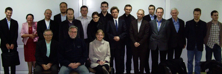
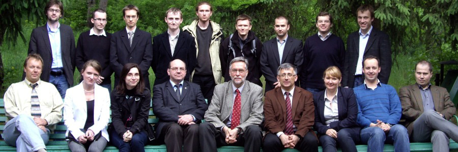
Author: Krzysztof BiernackiConference: Title